Shape Memory Alloy vs Voice Coil Motor OIS: Smartphone Camera Guide

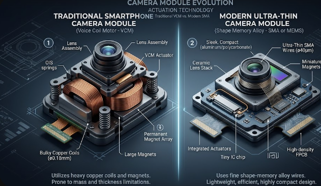
 Graphic comparing Shape Memory Alloy vs Voice Coil Motor OIS hardware inside a smartphone.

Have you ever wondered how your smartphone takes sharp photos even when your hands shake? The secret lies in Optical Image Stabilization (OIS). Recently, a big tech battle has emerged regarding Shape Memory Alloy vs Voice Coil Motor OIS systems in flagship phones. Manufacturers want to give you the best camera experience, but they use different mechanical methods to achieve it. Understanding this technology helps you make better buying decisions when comparing top-tier phone cameras.

The Mechanical Shift in Smartphone Cameras

For years, phone companies relied heavily on Voice Coil Motors (VCM) to stabilize lenses. A standard VCM setup uses heavy permanent magnets and copper wire coils. When electrical current passes through these coils, it creates a magnetic field that physically shifts the entire lens assembly to counteract your hand movements. While this method works well, it requires significant physical space and adds noticeable weight to the camera module.

In contrast, Shape Memory Alloy (SMA) actuators offer a completely different mechanical approach. Instead of bulky magnets, SMA technology uses specialized, hair-thin metal wires. These unique wires physically contract and expand when engineers apply a precise electrical current to them. This thermal reaction moves the lens rapidly and accurately, completely changing how engineers design modern mobile camera systems.

Weight and Size Benefits of Shape Memory Alloy vs Voice Coil Motor OIS

As smartphone sensors grow larger, space inside the phone body becomes extremely valuable. Because SMA completely eliminates bulky magnets and copper coils, it drastically reduces the physical footprint of the camera module. Therefore, manufacturers can pack massive image sensors into thin phones without creating huge, heavy camera bumps.

Furthermore, removing magnets solves a major engineering headache. Traditional VCM magnets can cause severe magnetic interference with neighboring lenses in a multi-camera array. For example, the magnet from a telephoto lens might disrupt the main camera. Because SMA actuators do not use magnets, they eliminate this risk entirely. Consequently, phone brands can place multiple high-powered cameras close together without performance issues.

Performance Battle: Multi-Axis Stabilization Limits

When we look at speed and accuracy, the difference between these two technologies becomes even clearer. A standard 4-wire SMA configuration allows for superior X and Y-axis stabilization. In addition, it enables active lens tilt, which corrects for rotational movements when you walk or run.

As a result, SMA systems react to micro-tremors from your hand with mathematically faster response times than spring-based VCM setups. Traditional VCM systems rely on tiny mechanical springs to hold the lens, which can wobble or lag during sudden movements. SMA wires pull tightly and release instantly, giving you incredibly smooth video and sharper low-light photos.

Final Thoughts on Shape Memory Alloy vs Voice Coil Motor OIS

Choosing a flagship phone often comes down to camera performance. While VCM remains a reliable and affordable choice for mid-range devices, SMA represents the future for premium photography. It gives you bigger sensors, lighter phone designs, and faster stabilization. To learn more about advanced mobile hardware and camera mechanics, check out Android Authority for deep dives into upcoming smartphone sensor tech.

References

  • Cambridge Mechatronics. (2024). Shape Memory Alloy (SMA) Technology for Smartphone Cameras.
  • IEEE Transactions on Magnetics. (2023). Comparison of Voice Coil Actuators and Smart Materials in Miniature Optical Systems.
  • Image Sensors World. (2025). Trends in Mobile Camera Modules: OIS and Actuator Evolutions.
Why PCIe 6.0 Retimers in AI Data Fabrics Are Critical for Speed

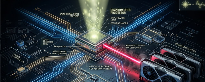
A detailed hardware diagram showing PCIe 6.0 retimers in AI data fabrics restoring signal strength between processors.

Artificial intelligence (AI) models require massive amounts of data to train and run efficiently. Because of this demand, modern data centers must move information between processors and memory at lightning speeds. This is why engineers now use PCIe 6.0 retimers in AI data fabrics to maintain clear communication lines. Without these specialized chips, high-speed servers would simply fail to process complex AI workloads.

The Physics Problem: Signal Integrity Bottlenecks

The latest PCIe 6.0 standard is incredibly fast, reaching transfer speeds of 64 Gigatransfers per second (GT/s). However, running data at this extreme frequency creates a massive physics problem known as signal degradation. When data travels at these speeds over standard motherboard copper traces, the electrical signal weakens almost immediately.

Consequently, the data distorts before it even reaches its destination. Think of this problem like shouting down a very long, windy tunnel. By the time your voice reaches the other side, the wind has turned your words into muffled, useless noise.

How Retimers Fix the Signal Loss

To solve this physical limitation, hardware architects install chips called retimers along the data path. These chips act like intelligent radio repeaters. First, the retimer catches the fading, noisy data signal before it degrades completely. Next, it cleans up the electrical noise and rebuilds the data packet. Finally, it retransmits a perfect, brand-new signal to the next component.

Therefore, using PCIe 6.0 retimers in AI data fabrics ensures that data travels across longer distances inside the server without any corruption. They are absolutely essential for keeping the internal data highway flowing smoothly.

Why Low Latency Matters for PCIe 6.0 Retimers in AI Data Fabrics

Speed is not just about bandwidth; it is also about latency. When you pool expensive GPU resources together for AI workloads, even a microscopic delay can ruin performance. Because of this issue, new hardware like Microchip’s XpressConnect retimers achieves an ultra-low latency of under 12 nanoseconds.

In the world of AI training, every single nanosecond counts. If one GPU stalls while waiting for data from another chip, the entire system slows down. This delay creates a bottleneck that wastes expensive computing power and increases operational costs.

By keeping latency below 12 nanoseconds, PCIe 6.0 retimers in AI data fabrics eliminate these microscopic data stalls. As a result, massive clusters of GPUs can work together seamlessly as if they were a single, giant processor.

Memory Disaggregation Specs: CXL 3.1 to the Rescue

Another major breakthrough in modern data centers is the Compute Express Link (CXL) 3.1 protocol. Traditionally, each processor socket has a strict physical limit on how much RAM it can hold. CXL 3.1 changes this rule entirely by introducing a concept called memory disaggregation.

This specific protocol allows multiple servers or GPUs to share a single, massive pool of external RAM. Instead of being trapped inside one server socket, the memory sits in an external pool that any processor can access on demand.

However, to connect these massive memory pools to your GPUs, you need an incredibly reliable connection. This is exactly where PCIe 6.0 retimers in AI data fabrics become valuable. They ensure the CXL 3.1 signals remain crisp and fast over the longer cables required for shared memory hardware.

Conclusion

Building efficient AI systems requires both massive bandwidth and perfect signal control. By combining CXL 3.1 memory pools with high-speed PCIe connections, data centers can handle the toughest AI workloads. Ultimately, deploying PCIe 6.0 retimers in AI data fabrics solves the core physics and latency issues of modern computing. For further technical details on how these components integrate into data centers, you can read more on the PCI-SIG Official Website.

References

  • Compute Express Link Consortium. (2023). CXL 3.1 Specification Features and Advancements.
  • Microchip Technology Inc. (2024). XpressConnect Retimers for PCIe 6.0 and CXL 3.0 Ultra-Low Latency Solutions.
  • PCI-SIG. (2022). PCI Express Base Specification Revision 6.0.

Are 8000Hz Polling Rate Peripherals Worth It? MCU and CPU Guide

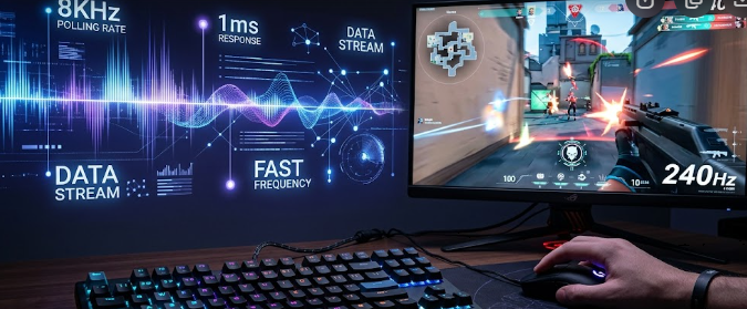
High-performance 8000Hz polling rate peripherals displayed next to a competitive esports gaming setup.

Competitive gamers always search for the fastest hardware to gain an advantage in esports. Recently, gaming brands started releasing 8000Hz polling rate peripherals, promising near-zero input latency. While these advanced mice and keyboards sound amazing on paper, they demand a massive amount of power from your computer. Consequently, you must understand the hidden hardware costs before upgrading your setup.

The Math Behind 8000Hz Polling Rate Peripherals

To understand this technology, we need to look at raw timing math. A standard gaming mouse usually operates at a 1000Hz polling rate. This means the mouse reports its position to your PC 1,000 times every second, which translates to once every 1 millisecond (ms).

In contrast, 8000Hz polling rate peripherals report data 8,000 times per second. Therefore, this rapid reporting slashes the update interval down to a microscopic 0.125ms.

1000Hz Polling Rate = 1 report every 1.0ms
8000Hz Polling Rate = 1 report every 0.125ms

This rapid reporting creates an incredibly dense stream of positional data. As a result, your cursor movements feel significantly smoother and more responsive on your screen. However, you will only notice this microscopic difference under very specific hardware conditions.

Why Monitor Refresh Rates Create a Visual Bottleneck

Many gamers buy 8000Hz polling rate peripherals expecting an instant visual upgrade. Unfortunately, your monitor can create a massive visual bottleneck that negates the benefits.

If you use a standard 60Hz monitor, your screen only updates 60 times a second, or once every 16.67ms. Even a standard 144Hz gaming monitor only updates every 6.94ms. Therefore, these slower monitors physically cannot display the extra positional updates that an 8K mouse sends every 0.125ms.

Spec-Matching Guide for High Refresh Displays

To actually see the benefits of this technology, you need an ultra-high refresh rate display. Specifically, displays pushing 360Hz, 480Hz, or higher are physically necessary to render the smoother tracking data.

Monitor Refresh RateTime Between Screen Frames8K Polling Updates Per Frame
60Hz16.67 ms~133 updates
144Hz6.94 ms~55 updates
240Hz4.17 ms~33 updates
360Hz2.78 ms~22 updates

For example, a 360Hz monitor updates its frame every 2.77ms. While it still cannot show every single one of the 8,000 updates, it matches the dense data stream much better than slower screens. Thus, upgrading your mouse without a high-end monitor completely wastes the hardware’s potential.

Internal MCU Constraints of 8000Hz Polling Rate Peripherals

Transmitting thousands of data packets every second requires serious processing power inside the device itself. Standard gaming mice use basic, low-power microcontrollers to handle data tracking.

Conversely, 8000Hz polling rate peripherals require dedicated, high-performance microcontrollers (MCUs). This advanced internal hardware must compress and process the intense data stream before sending it through the USB cable. As a result, these advanced devices often cost significantly more and consume far more battery power if they use a wireless connection.

CPU Overhead Penalties and Game Performance

The real hidden cost of 8000Hz polling rate peripherals falls directly on your computer’s processor. Your CPU must process all 8,000 incoming data packets every single second.

This heavy workload demands continuous, intense CPU cycles from the host PC. If you play demanding first-person shooters, your processor is already working incredibly hard to render the game frames. Consequently, the added tracking data can easily overload older or mid-range processors.

How System Overload Affects In-Game Framerates

When your processor struggles with the sudden flood of mouse data, you will experience performance issues. Many players notice sudden, jarring drops in their in-game framerates (FPS) whenever they move their mouse quickly.

Furthermore, this heavy CPU overhead can cause micro-stuttering, which completely ruins your aiming consistency. Therefore, a hardware upgrade meant to give you a competitive advantage might actually hurt your gameplay if your CPU cannot handle the stress.

Final Recommendations for Competitive Gamers

In conclusion, 8000Hz polling rate peripherals offer groundbreaking latency reduction on paper. However, you must ensure your entire system is ready for the upgrade before purchasing them.

You absolutely need a top-tier modern CPU and a monitor that pushes at least 360Hz to truly enjoy the smoother tracking. If you use older or mid-range hardware, sticking to a stable 1000Hz or 2000Hz rate will provide a much better, stutter-free gaming experience. For a deeper look at how input latency and peripheral refresh rates affect competitive gaming performance, you can read the comprehensive analysis on Blur Busters.

References

  • Razer Inc. (2023). “Razer HyperPolling Technology: True 8000Hz Polling Rate Whitepaper.”
  • Blur Busters. (2021). “The Amazing Benefits of High Polling Rates (1000Hz vs 8000Hz).”
  • RTINGS Hardware Reviews. (2024). “Mouse Polling Rate: Does It Matter For Gaming?”

 PCIe Gen 6.0 Clock Jitter: The Guide to 64 GT/s Stability

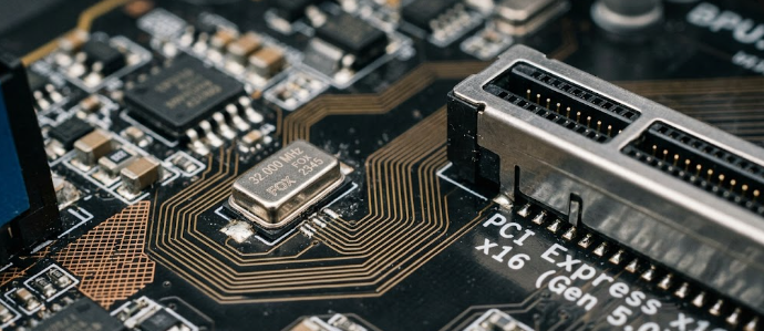
 High-end motherboard crystal oscillator demonstrating the impact of PCIe Gen 6.0 clock jitter on data transfer.

The computer hardware industry advances rapidly, and the jump to new data speeds naturally brings new challenges. Today, PC builders and enterprise experts closely watch the transition to next-generation components. One massive hurdle stands in the way of achieving perfect 64 GT/s speeds. Engineers call this specific problem PCIe Gen 6.0 clock jitter. When you upgrade your system, you rightfully expect flawless performance. However, microscopic timing errors can easily ruin data transmission. Therefore, understanding this concept helps you make much smarter choices when buying premium hardware.

The Tolerance Shrink of PCIe Gen 6.0 Clock Jitter

Previous generations of PCIe used simple signaling methods. Now, the new standard doubles data rates to an incredible 64 GT/s per lane. To achieve this, the architecture uses a technology called PAM4 signaling. PAM4 essentially packs more data into every electrical signal, but it severely shrinks the acceptable timing margin. Consequently, the system leaves almost no room for error. If the timing shifts even slightly, the entire connection destabilizes.

Because of this shrinking margin, the system clock must run flawlessly at all times. In fact, the acceptable PCIe Gen 6.0 clock jitter has dropped below 100 femtoseconds (fs). For context, one femtosecond equals one-quadrillionth of a second. Imagine a musician playing alongside a mechanical metronome. If the metronome ticks inconsistently, the musician misses the beat. Similarly, if your motherboard clock ticks inconsistently, the processor drops the data.

How RMS Metrics Measure PCIe Gen 6.0 Clock Jitter

To track these incredibly tiny errors, hardware engineers use Root-Mean-Square (RMS) metrics. RMS jitter calculates the average deviation of the clock signal over time. A motherboard clock generator sends millions of electrical pulses every single second. Ideally, each pulse should land at the exact right microsecond. Unfortunately, real-world electronics always experience microscopic variations in pulse timing. These variations directly represent the actual jitter in the system.

Furthermore, high RMS jitter creates devastating consequences for high-speed data transfer. When the timing shifts too much, fast-moving data packets literally crash into each other. This physical overlap scrambles the digital information completely. As a result, the motherboard triggers severe cyclic redundancy check (CRC) errors. CRC errors force the hardware to resend the exact same data, which immediately kills your performance and ruins the benefit of the 64 GT/s speed.

Fighting PCIe Gen 6.0 Clock Jitter with Premium Components

Naturally, this strict specification drastically changes how manufacturers build modern motherboards. You simply cannot achieve a stable 64 GT/s connection with cheap, basic parts. To conquer PCIe Gen 6.0 clock jitter, motherboard brands must adopt premium component requirements. First, they install highly specialized, low-jitter crystal oscillators. These expensive oscillators maintain the perfect, steady heartbeat needed for PAM4 signaling.

Additionally, manufacturers must completely upgrade the physical circuit boards. Standard boards often interfere with high-speed signals. Therefore, premium brands now use server-grade, low-loss printed circuit boards (PCBs). These advanced PCBs protect the fragile data from background electrical noise. Ultimately, extreme overclockers and builders must pay close attention to these components. Buying a cheap motherboard will severely throttle your next-gen graphics cards and storage drives.

In summary, pushing consumer hardware to 64 GT/s requires incredible electronic precision. You must understand PCIe Gen 6.0 clock jitter to truly appreciate the engineering behind next-generation motherboards. As you prepare your next extreme PC build, always verify the quality of the clock generators and the PCB material. For more detailed technical insights on PCIe architecture and electrical testing, you can read further on the PCI-SIG official website.

References

  1. PCI-SIG. “PCI Express 6.0 Specification.” PCI-SIG Publications, 2022.
  2. Tektronix. “Understanding and Characterizing Timing Jitter.” Tektronix Technical Brief.
  3. Keysight Technologies. “PAM4 Signaling in High-Speed Digital Systems.” Keysight Hardware Engineering Papers.

 Why Dual-Cell Smartphone Batteries Power 120W+ HyperCharging

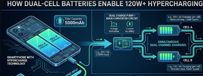
Dual cell pnone batteries enable hypercharging

Smartphone charging speeds have increased rapidly over the last few years. If you are comparing mobile tech metrics on 2026 flagship devices, you have likely seen terms like 120W or 150W HyperCharging. Many users wonder how premium phones handle this massive power without exploding or degrading. The secret lies in an innovative engineering setup inside the phone. Manufacturers no longer use traditional single-cell power packs to achieve these speeds. Instead, modern flagships rely on Dual-Cell Smartphone Batteries to safely rewrite the rules of mobile power delivery.

Splitting the Voltage: The Core Engineering Specification

To understand why traditional setups fail at ultra-fast speeds, we must look at how electricity moves. Pushing 120W of power into a single battery cell creates massive electrical resistance. High resistance always generates extreme heat, which damages lithium-ion cells very quickly. Therefore, engineers had to redesign the internal architecture of modern mobile devices.

Instead of using one large, single block, manufacturers now split the battery into two physically separate sections. These two parts connect in a series circuit inside the phone chassis. This series connection changes how the phone handles the incoming electrical force. By utilizing Dual-Cell Smartphone Batteries, the device can split the overall voltage requirement across two paths. This design choice prevents a single cell from taking the entire workload alone.

The Physics of Series Connections

When you connect two power cells in a series, the total voltage doubles while the current remains steady. A standard single smartphone cell usually maxes out at a charging voltage of about 4.45V. If you attempt to force 120W into that single cell, the electrical current must be extremely high.

High current requires thick internal wires and creates an unbearable thermal load for a thin mobile device. Splitting the battery into two separate pieces instantly solves this physical limitation. The system treats the dual cells as a single high-voltage system during the initial power intake stage. As a result, the phone can accept much higher power inputs from the wall adapter safely.

Charge Pump Math: How 120W and 150W Delivery Works

The magic of hyper-fast charging requires perfect cooperation between your wall charger and your phone. A 120W hyper-charger does not just blindly dump raw electricity into your device. Instead, it sends electricity at a very specific high-voltage and low-current ratio. For example, a 120W wall brick typically outputs 20 volts (V) at 6 amperes (A).

20V × 6A = 120W (Total Output Power)

If 20V entered a standard phone battery directly, it would instantly destroy the delicate internal components. This is where specialized internal microchips, known as charge pumps, come into play. These advanced silicon chips act as highly efficient DC-to-DC voltage converters inside your handset.

Breaking Down the Internal Math

When the 20V at 6A current enters the phone, the internal charge pumps instantly alter the electrical metrics. The charge pumps utilize a specific 2:1 step-down ratio to alter the incoming power safely. This means the chips cut the incoming voltage precisely in half while keeping the current stable.

20V / 2 = 10V (Voltage after Charge Pump step-down)

Consequently, the power transforms from 20V at 6A down to a much safer 10V at 6A. Because the Dual-Cell Smartphone Batteries are connected in a series, this 10V stream distributes evenly. Each individual cell receives exactly 5V at 6A simultaneously.

Cell 1: 5V × 6A = 30W
Cell 2: 5V × 6A = 30W
Total Combined System Power = 60W per charge pump channel (doubled via dual channels to 120W)

This clever mathematical distribution allows both cells to fill up at the exact same time. The phone achieves extreme speeds because it charges two separate tanks at a safe, moderate pace.

Thermal and Degradation Specs: Beating the Heat

Heat is the ultimate enemy of battery health and long-term capacity retention. When a phone gets too hot during a charging session, the operating system triggers thermal throttling. Throttling forces the charging speed to drop drastically to let the device cool down.

Traditional single-cell phones throttle very early in the charging cycle because they heat up so quickly. Utilizing Dual-Cell Smartphone Batteries minimizes this internal resistance significantly. Lower resistance means the device generates far less thermal waste during high-wattage transfers.

Maintaining Peak specified Wattage

Because the dual-cell design keeps temperatures low, your phone can sustain peak wattage for much longer periods. Instead of throttling down after just two minutes, 2026 flagships can hold high speeds deep into the charging cycle.

Furthermore, minor design tweaks like Multiple Tab Winding (MTW) reduce internal resistance even more by shortening the path electricity travels. This means you can charge from zero to 100% in under twenty minutes without cooking the motherboard.

Long-Term Battery Health and Lifespan

Many buyers worry that 120W HyperCharging will ruin their battery health within a single year of use. Thankfully, the dual-cell configuration protects the lifespan of your device. Because each cell only experiences a fraction of the total stress, degradation slows down.

Most modern flagship devices using this tech retain up to 80% of their original capacity after 800 full cycles. This longevity matches or exceeds older, slower charging standards. You get the benefit of ultra-fast speeds without sacrificing the long-term usability of your premium smartphone. For a deeper technical dive into how advanced battery chemistries handle rapid power transfers, you can read the comprehensive Android Central Battery Technology Guide.

References

  • ChargerLAB. (2023). Single-Cell vs. Dual-Cell Batteries: What’s the Difference? * Halo Microelectronics. (2022). Powering Smartphones with 2:1 Charge Pump Direct Charger IC. * Xiaomi Global. (2021). How Does 120W Xiaomi HyperCharge Work? Inside the Technology.

VESA ClearMR 14000: The Ultimate Guide to Display Motion Blur

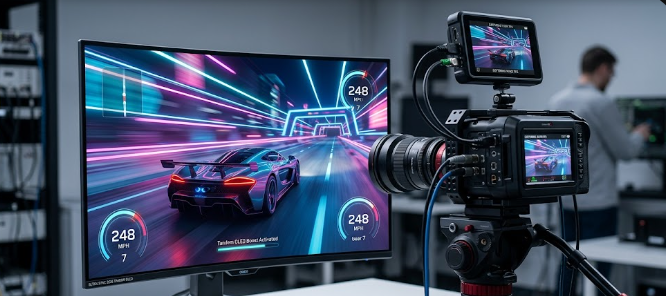
 A high-speed digital camera measuring VESA ClearMR 14000 performance on a gaming monitor.

Are you tired of buying a gaming monitor that promises lightning speeds but still delivers a blurry mess during fast action? You are certainly not alone. Therefore, you need to understand the VESA ClearMR 14000 standard. This brand-new metric is changing how we buy screens today. Previously, companies sold monitors using confusing terms that did not match real-world viewing. However, the VESA ClearMR 14000 certification guarantees that the screen handles motion perfectly. Whether you play competitive games or watch fast-moving sports, this standard helps you pick the right display. In this article, we will explore why this new rating matters. Furthermore, we will show you how it easily beats older measurement methods.

Why Outdated Metrics Fail Gamers

For many years, manufacturers used the Gray-to-Gray (GtG) metric to sell monitors. You probably saw boxes proudly showing “1ms GtG.” Unfortunately, this old specification frequently misleads buyers. GtG only measures how fast a single pixel changes from one shade of gray to another. Consequently, it completely ignores how your eyes actually see a moving picture full of bright colors.

Manufacturers often use software tricks to speed up these gray-to-gray transitions. As a result, you might buy a “1ms” monitor and still experience terrible motion blur during a fast gaming match. To fix this obvious problem, the display industry needed a better testing method. That is exactly where the new testing standard steps in to save the day.

How VESA ClearMR 14000 Measures Real Blur

Unlike old methods, the VESA ClearMR 14000 standard uses advanced physical tools to test screens. Testers point high-speed digital cameras and precise colorimeters directly at the monitor. Next, they record exactly how the pixels handle fast-moving objects on the screen. This rigorous process measures true motion blur in a way that perfectly matches human eyesight. Consequently, you get a realistic score based on the Clear Motion Ratio (CMR).

So, what does this specific tier mean for your eyes? When a monitor earns a VESA ClearMR 14000 badge, it delivers an incredibly sharp picture. Specifically, this tier dictates that sharp pixels outnumber blurry pixels by a massive factor of 135 to 145 times. For example, if you watch a fast-moving soccer ball, you will see exactly one slightly blurry pixel for every 135 perfectly clear ones.

Panel Technologies Reaching VESA ClearMR 14000

Achieving this elite certification requires serious hardware power. Today, the latest 2026 Tandem OLED monitors easily match up against these demanding tiers. Because OLED pixels create their own light, they turn on and off almost instantly. Furthermore, modern high-zone Mini-LED monitors also perform exceptionally well in these tests. These advanced Mini-LED panels use thousands of tiny lights to control brightness with incredible speed.

Both of these modern panel architectures feature rapid pixel response profiles. Consequently, they easily earn higher ClearMR certifications from testers. When you compare an older LED screen to a new 2026 Tandem OLED, the visual difference feels massive. The newer technology eliminates the annoying ghosting effect completely. Therefore, your competitive games look smoother, sharper, and much more realistic.

Wrapping Up Your VESA ClearMR 14000 Upgrade

Upgrading your monitor is a big investment, so you should always look for accurate performance numbers. In conclusion, you should ignore the outdated gray-to-gray times and look for the VESA ClearMR 14000 logo instead. This modern standard gives you total peace of mind and guarantees a crystal-clear image. As you search for your next competitive gaming screen, keep this powerful metric in mind to ensure you get the best value. Finally, if you want to dive deeper into how professionals test screen clarity and motion reduction, you can read more at Blur Busters.

References

  • Video Electronics Standards Association (VESA). (2026). ClearMR Display Standard Specifications.
  • Blur Busters. (2026). Understanding Motion Blur Reduction and Display Metrics.