Biometric security has evolved rapidly over the last few years. While fingerprint scanners and facial recognition are highly common, tech enthusiasts now demand stronger privacy measures. Hackers can easily trick standard scanners using high-resolution photos or advanced digital deepfakes. Because of these rising threats, top hardware manufacturers are shifting toward a much more secure alternative. Near-Infrared Vein Recognition has officially emerged as the gold standard for premium device security in 2026.
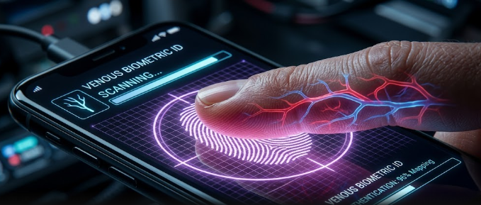
This cutting-edge technology looks beneath the surface of your skin to verify your identity. Instead of analyzing your external features, it scans the unique patterns of your blood vessels. This approach offers a massive leap forward in digital privacy and hardware security.
Understanding the Sub-Dermal Optical Layer
The true magic of this technology happens hidden away from the naked eye. Traditional scanners only capture what is on the surface of your skin. In contrast, Near-Infrared Vein Recognition utilizes specialized light arrays to map your internal anatomy. These tiny sensors emit a specific wavelength of near-infrared light, which usually peaks right at 850 nanometers.
When this light hits your hand, your skin absorbs and reflects it in a unique way. Specifically, the deoxygenated hemoglobin in your veins absorbs the infrared light. This absorption creates a dark, highly detailed map of your sub-dermal blood vessels. The sensor captures this hidden image and converts it into an encrypted biometric key. Because your vein structure is entirely internal, nobody can copy or steal your pattern.
Unbeatable Accuracy and Lower False Acceptance Rates
Security professionals closely track a metric called the False Acceptance Rate (FAR). This rate measures how often a security system accidentally grants access to an unauthorized user. Standard 2D or 3D facial mapping systems have notable vulnerabilities. For example, a high-quality 3D mask or a sophisticated deepfake can sometimes trick a front-facing camera.
Fortunately, Near-Infrared Vein Recognition delivers a vastly superior mathematical security profile. These advanced systems routinely achieve a near-zero FAR of less than 0.0001%. This means the odds of a stranger unlocking your device are literally less than one in a million. Consequently, it provides a much safer environment for mobile banking, crypto wallets, and highly sensitive corporate data.
Advanced Liveness Detection Hardware
Experienced hackers often try to bypass biometric scanners using static models or artificial duplicates. However, modern vein scanners completely eliminate this risk through active hardware checks. The sensor does not simply look at a static image of your veins. Instead, the hardware actively monitors your body for signs of biological life during every single scan.
The optical module instantly measures your pulse and blood oxygen saturation (SpO2) levels. It ensures that blood is actively flowing through the veins before it grants access. Therefore, an attacker cannot bypass the system using a synthetic mold, a printed photo, or a non-living duplicate. This real-time liveness detection makes the hardware practically impossible to spoof.
Overcoming Modern Integration Constraints
Enthusiasts love slim devices, which creates a major challenge for hardware engineers. Embedding complex optical modules into ultra-thin laptop bezels requires incredible engineering skill. Furthermore, fitting these sensors into the sub-display stack of premium smartphones demands precise space management.
Engineers have successfully shrunk these infrared emitters and receivers into microscopic packages. They can now layer these components directly beneath vibrant OLED screens without affecting display quality. As a result, users get unmatched security without sacrificing the sleek, bezel-less designs of modern flagship phones.
If you want to read more about the physics behind optical light absorption and blood monitoring, check out the detailed scientific analysis on the IEEE Xplore Digital Library.
References
- Biometric Research Group. (2025). Next-Generation Sub-Dermal Authentication Standards.
- Journal of Electronic Engineering. (2026). Shrinking Near-Infrared Sensors for Mobile Display Stacks.
- Global Security Metrics. (2026). Comparative Analysis of FAR in Facial Recognition vs. Vein Scanners.