Rice is a favorite staple food on many dinner tables around the world. However, eating plain white rice, Jollof rice, or fried rice by itself can lead to noticeable health challenges. Plain rice provides quick-burning carbohydrates, but it lacks sufficient dietary fiber, protein, and essential micronutrients. Consequently, your body digests it too fast, causing sharp blood sugar spikes followed by sudden energy crashes. Fortunately, you can easily transform popular rice dishes into complete, balanced meals that keep you full and energized throughout the day.
Use the Half-Plate Rule to Transform Popular Rice Dishes
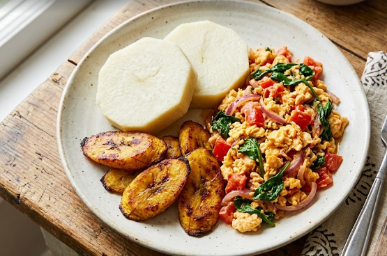
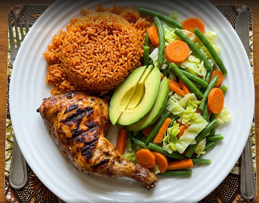
First, you should adopt the simple half-plate rule during your meal preparation. This method requires you to fill half of your plate with fresh or cooked vegetables before adding any rice. For example, you can choose steamed carrots, green beans, sliced cabbage, or a fresh garden salad. Because vegetables contain high amounts of natural fiber, they slow down carbohydrate digestion in your stomach. As a result, your body releases glucose into the bloodstream at a steady pace, preventing sudden blood sugar spikes.
Add Protein Anchors for Sustained Energy
Next, you must pair your rice with a strong protein source to build a truly balanced plate. Protein acts as an anchor because your stomach takes longer to break it down than simple carbohydrates. Therefore, adding quality protein helps maintain your muscle mass while promoting long-lasting fullness. Great choices include grilled mackerel (titus), hard-boiled eggs, skinless chicken breast, or lean goat meat. When you add these options, you effectively balance the quick carbohydrates in the rice with steady, slow-releasing energy.
Apply Smart Cooking Tweaks
In addition to adding protein and fiber, you can improve meal quality by tweaking your cooking methods. Traditional Jollof and fried rice recipes often use large amounts of vegetable oil. However, you can easily reduce the amount of cooking oil without losing any rich flavor. Furthermore, you should substitute deep frying with baking or grilling for your side items. For instance, grilling your chicken or fish instead of deep frying cuts down unneeded calories and harmful fats significantly.
Upgrade to Healthy Fat Sources
Finally, focus on adding beneficial fats to your meal instead of relying on heavy, oil-laden stews. Healthy fats protect your heart and help your body absorb essential vitamins like vitamins A, D, and E. For instance, you can add fresh avocado slices or sprinkle toasted seeds over your rice dish. These wholesome fats provide a rich texture, enhance natural flavors, and support your long-term health.
By making these simple adjustments, you can enjoy your favorite rice dishes while giving your body the nutrients it needs. You do not have to give up your favorite foods to stay healthy. Instead, balance your portion sizes, include fresh vegetables, choose lean proteins, and cook with lighter methods. For additional guidance on structuring a balanced diet, check out the interactive guidelines on the Harvard T.H. Chan School of Public Health website.
References
- Harvard T.H. Chan School of Public Health. (2021). The Healthy Eating Plate.
- Slavin, J. L. (2005). Dietary fiber and body weight. Nutrition, 21(3), 411-418.
- American Diabetes Association. (2023). Understanding Carbohydrates and Blood Sugar Management.