Smartphone cameras are improving at a very fast pace. You can now take beautiful photos that look like they came from a professional camera. Most of this magic happens inside the image sensor. Sony is the leading company in this space. They recently introduced a new brand of sensors called LYTIA. Many new flagship phones use these chips to capture stunning images. In this article, we will look at the internal technology of these chips. This guide will help you understand the core details as we ensure the complex Sony LYTIA Sensor Specs Demystified for your next phone purchase.
What is the Stacked BSI Architecture?
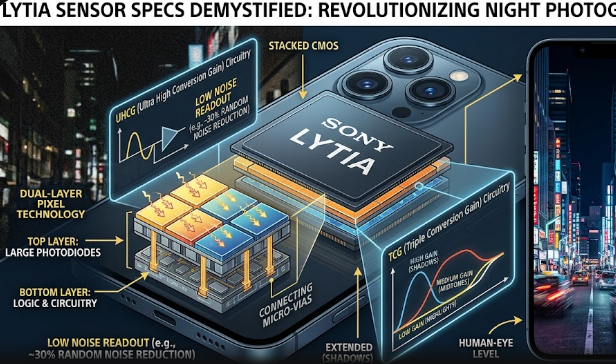
Traditional smartphone sensors place the light-capturing parts and the electrical wires on the exact same flat surface. This layout creates a major design problem. Because they share the same space, the light-gathering area must stay small. Sony solved this issue by creating a smart design. They call this design the Stacked Back-Illuminated architecture.
In this design, Sony physically separates the light-capturing photodiodes from the readout transistors. They stack them on two distinct silicon layers instead of keeping them side by side. The top layer holds only the photodiodes to maximize the surface area for gathering light. The bottom layer holds the transistors that read the signal. This layout doubles the amount of light the sensor can hold at one time. It prevents your photos from looking blown out in bright sunlight. It also keeps your images detailed.
Optical Formats and Phone Footprint
You might think that a more powerful camera requires a massive camera bump on the back of your phone. However, this new stacking technology changes the rules of phone design. It changes how we look at the relationship between sensor performance and physical size.
“By separating the layers, Sony can pack massive light-gathering power into a very small area.”
This clever setup allows a highly capable 50MP sensor to fit into a relatively compact 1/1.56-inch or 1/1.4-inch optical format. For example, sensors like the LYT-700 and LYT-808 use this design to give you flagship-level photos. They help phone makers maintain a thin smartphone chassis without adding a massive camera bump. You get the power of a giant camera sensor without carrying a heavy, bulky device in your pocket.
Native vs Effective Pixel Size Math
When you read the technical sheets for these sensors, you will see terms like pixel binning. This process uses advanced math to improve your night photos. A 50-megapixel sensor has millions of tiny individual pixels on its surface.
[Native Pixel: 1.0 μm] + [Native Pixel: 1.0 μm]
–> Combine into –> [Effective Super-Pixel: 2.0 μm]
[Native Pixel: 1.0 μm] + [Native Pixel: 1.0 μm]
These sensors have a native pixel size of 1.0 micrometer. That size is great for bright daylight because it captures sharp details. However, small pixels struggle in low-light environments because they cannot catch enough light. To fix this, the sensor uses a Quad Bayer filter for 4-in-1 pixel binning. This math combines four neighboring pixels into one large block.
This process creates an effective 2.0 micrometer super-pixel. This transformation drastically improves the signal-to-noise ratio. The larger super-pixel acts like a wide window that lets in massive amounts of light. This step ensures your evening photos stay bright and clear.
Ultra High Conversion Gain Technology
The final piece of the puzzle is a specific circuit technology called Ultra High Conversion Gain. This circuit acts like a clean amplifier for the electrical signals inside the camera. When light hits the sensor, it turns into an electrical charge. The sensor must convert this charge into a voltage signal to create your digital photo.
The Ultra High Conversion Gain circuits translate this charge to voltage efficiently. This process is very important when you shoot pictures in dark rooms or outside at night. It targets and eliminates the grainy, random noise usually found in night photography. Instead of amplifying the background static, it boosts only the pure image signal. This gives you deep blacks and smooth colors in dark areas.
If you want to read more about advanced mobile camera sensor designs, you can check out this detailed industry analysis on image sensor architectures.
References
- Sony Semiconductor Solutions Group. (2023). 2-Layer Transistor Pixel Technology for Mobile CMOS Image Sensors.
- Sony LYTIA Product Lineup Specifications. (2024). LYT-700 and LYT-808 Hardware Documentation. * Digital Photography Review. (2024). Understanding Quad Bayer Sensors and Pixel Binning Math.