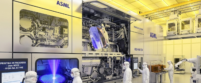
PC builders, tech speculators, and engineering enthusiasts always look forward to the next big leap in computing power. Today, companies like Intel and TSMC race to build faster and smaller chips. To achieve this, they rely on cutting-edge manufacturing tools. The most important tool driving the future of 2026 silicon is High-NA EUV lithography. This groundbreaking technology changes how engineers print microscopic circuits onto silicon wafers. Consequently, it unlocks a new era of processing power for our computers and smartphones.
Furthermore, this leap in technology is not just a minor upgrade. It requires a complete redesign of the optical systems that print microchips. Let us explore the technical specifications behind this massive shift in semiconductor fabrication.
The Numerical Aperture Jump in High-NA EUV Lithography
First, we must understand what Numerical Aperture (NA) means in optical lithography. Simply put, NA measures how well a lens or mirror system can collect and focus light. Think of it like the aperture on a professional camera. A larger aperture gathers more light, which allows the camera to capture sharper, more detailed photos.
Historically, chipmakers relied on standard Extreme Ultraviolet (EUV) systems with a 0.33 NA. However, the new generation of High-NA EUV lithography pushes this number to a 0.55 NA. This significant jump allows the internal lasers to print sub-10nm optical resolutions directly onto silicon wafers. Therefore, manufacturers can pack billions of additional transistors into the exact same physical space, making our daily devices dramatically faster and much more power-efficient.
Anamorphic Lenses and the Field Size Trade-Off
Despite the incredible benefits, achieving a 0.55 NA creates a massive physical challenge. The mirrors required to capture and focus this light are absolutely massive. Because these mirrors take up so much space inside the machine, engineers had to change the shape of the lenses. They introduced anamorphic lenses.
Specifically, anamorphic lenses magnify light at different ratios on the X and the Y axis. For example, imagine looking into a funhouse mirror that stretches your reflection horizontally but keeps your vertical height exactly the same. Because the system squishes the light asymmetrically to fit the massive mirrors, it creates a serious trade-off. This design cuts the printable wafer field size entirely in half, reducing the maximum print area down to just 26 mm x 16.5 mm.
Why High-NA EUV Lithography Demands Die Stitching
Because the printable area shrinks so drastically, chip designers face a major hurdle. Modern consumer hardware, like massive artificial intelligence processors and high-end gaming GPUs, feature incredibly large die sizes. Consequently, the new machines cannot print these giant chips in one single exposure.
To solve this problem, manufacturers use a clever technique called die stitching. Since the field size is smaller, engineers print two separate halves of a microchip side-by-side. Next, they fuse these two halves seamlessly together on the silicon wafer. You can compare this to a tailor sewing two pieces of fabric together to create a large, seamless blanket. Ultimately, this stitching specification ensures that High-NA EUV lithography can still produce the massive chips required for next-generation PC builds and AI data centers.
In conclusion, understanding these intricate manufacturing details helps us appreciate the engineering miracles happening inside our computers. As Intel and TSMC adopt these machines, we will see entirely new classes of hardware hit the market. If you want to dive even deeper into the physics of how these advanced lasers operate, you can read more about it on the ASML official technology page.
References
- ASML. (2024). High-NA EUV (EUV 0.55 NA) Lithography. ASML Corporate Website.
- IEEE Spectrum. (2023). How High-NA EUV Will Keep Moore’s Law Alive. IEEE.
- Intel Newsroom. (2024). Intel’s Adoption of High-NA EUV for Future Nodes. Intel Corporation.