Gamers and PC builders always want faster processors to run heavy workloads. To achieve this goal, AMD introduced an incredible hardware innovation known as AMD 3D V-Cache technology. Consequently, modern X3D processors deliver unmatched gaming performance by changing how engineers build CPUs. In this article, we will look at the physical hardware and advanced engineering driving this design.
Moving Upward with AMD 3D V-Cache Technology
Traditionally, chip makers expanded processor size horizontally across a flat plane. This older method represents planar expansion. However, spreading components out across a flat surface creates major problems. It increases the physical size of the chip and forces data to travel longer distances. As a result, latency increases and slows down communication between the core and memory.
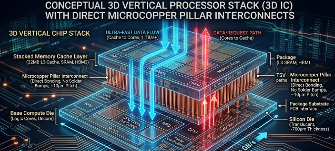
To solve this issue, AMD chose a radical vertical approach. Instead of expanding outward, engineers stack a 64MB SRAM cache die directly on top of the CPU compute die (CCD). Therefore, the processor gains massive memory capacity without expanding its horizontal footprint. This vertical shift keeps data paths incredibly short, which slashes latency and speeds up performance dramatically.
The Power of Direct Cu-Cu Bonding Specs
Older chip designs connected stacked layers using tiny traditional solder bumps, which engineers call micro-bumps. Unfortunately, micro-bumps take up too much space and create high electrical resistance. They also limit how close connection points can be. To overcome this limitation, AMD uses a cutting-edge hybrid bonding process called direct copper-to-copper (Cu-Cu) bonding.
This new design completely eliminates traditional solder bumps. Instead, the copper pads of the top layer touch the copper pads of the bottom layer directly. This precise method allows for a sub-10 μm interconnect pitch, meaning the connection points sit incredibly close together. Ultimately, AMD 3D V-Cache technology benefits from drastically lowered electrical resistance and vastly superior power efficiency.
Vertical Data Highways in AMD 3D V-Cache Technology
How do the CPU cores talk to this newly stacked memory so quickly? The answer lies in Through-Silicon Vias, or TSVs. TSVs act as microscopic vertical data highways that drill straight through the silicon layers.
Because these pathways are so tiny and numerous, they provide massive data lanes. Therefore, the CPU cores can access the stacked L3 cache at over 2 TB/s of bandwidth. This extreme speed ensures that the processor never starves for data during heavy gaming or intense workloads.
Managing Heat in Advanced 3D Processors
Stacking silicon layers creates amazing performance, but it also creates severe thermal challenges. When you place a cache die directly over hot CPU cores, you trap heat underneath. Consequently, these X3D chips have stricter maximum temperature limits, which engineers call Tjmax, compared to standard 2D processors.
To protect the hardware, AMD applies lower voltage ceilings to these chips. Extreme overclockers must respect these boundaries because excessive voltage can permanently damage the bonded layers. Therefore, choosing a high-quality cooling system is absolutely vital if you want to get the most out of AMD 3D V-Cache technology.
The Future of Processor Design
In conclusion, AMD has revolutionized CPU architecture by building upward rather than outward. By combining direct Cu-Cu bonding with microscopic vertical data paths, they have rewritten the rules of gaming performance. If you want to dive deeper into the official hardware specifications, you can read more about CPU architectures on the AnandTech CPU Tech Section.
References
- AMD. (2026). AMD 3D V-Cache™ Technology Drives Density and Energy Efficiency Leadership. AMD Tech Insights.
- Avaq Semiconductor. (2026). AMD 3D V-Cache Technology Explained: A Breakthrough in 3D Chip Integration for HPC and Gaming.
- Yole Group. (2022). AMD 3D V-Cache with TSMC SoIC 3D Packaging Teardown Report.